|
DCIP2D:
|
|
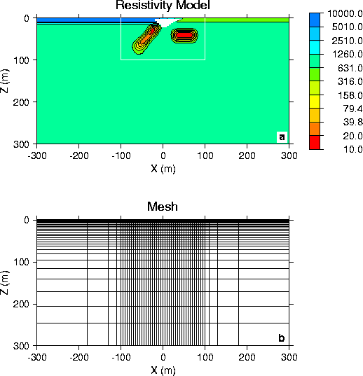
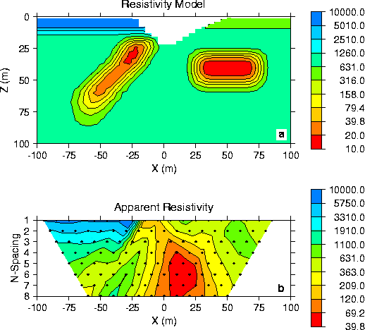
Previous Page (Introduction) | Next Page (General Methodology for inverting DC and IP data) The forward modelling for the DC potentials and IP apparent chargeabilities is accomplished using a finite difference technique to solve equation (2). The program which performs this calculation is DCIPF2D. To illustrate the DC resistivity forward modelling algorithm we generate synthetic data that would be acquired over the 2D conductivity structure shown in Fig 2a. The model region consists of a 10 meter thick overburden having conductivity of 0.1 mS/m on the left and 2 mS/m on the right. A V-shaped valley is cut out to simulate the surface topography. Two conductors are buried in the underlying background of 1 mS/m. On the left, a dipping conductor having a dip of 135o and conductivity of 100 mS/m is buried at a depth of 20 m to the top. On the right, a 50 meter long, 20 meter thick conductive block of 100 mS/m is buried at a depth of 25 meters. Rather than keep the model as discrete blocks we have attempted to make it more geologically realistic by applying a smoothing filter to the model. The model is divided into 48 cells in the x-direction and 27 cells in the z-direction so there are 1296 cells. The finite difference mesh is shown in Fig 2b. In the survey, surface electrodes are located every ten meters in the interval x=(-100,100) meters. We compute the potential differences from a pole-dipole array with the potential electrodes on the right. Our designation for this is PDR (Potential Dipole Right). There are 19 possible current electrode locations and we record the data for each electrode to a maximum n-spacing of 8. The observed data set consists of 124 potential difference values. It is our intention to use these data as input to an inversion. In order to make them more realistic we contaminate each datum by adding Gaussian noise having a standard deviation equal to 5% of the true potential. The apparent resistivity pseudo-section is shown in Fig 3b. That figure can be compared with the conductivity model in Fig 3a. There is some manifestation of the horizontal conductive block but much of the conducting "pant-leg" seen is really the result of the near surface variation of conductivity and topography. The forward modelling for the IP data is also performed with the program
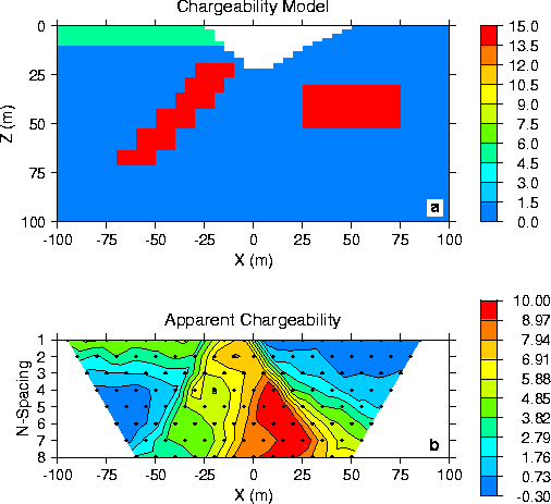
DCIPF2D. To calculate IP data, the program performs two DC forward
modellings and the IP data are generated by the operations indicated in
equation (6). For a synthetic example we choose the chargeability model
in Fig 4a. It consists of a chargeable layer at the surface with
Previous Page (Introduction) | Next Page (General Methodology for inverting DC and IP data) |
 =0.05
=0.05